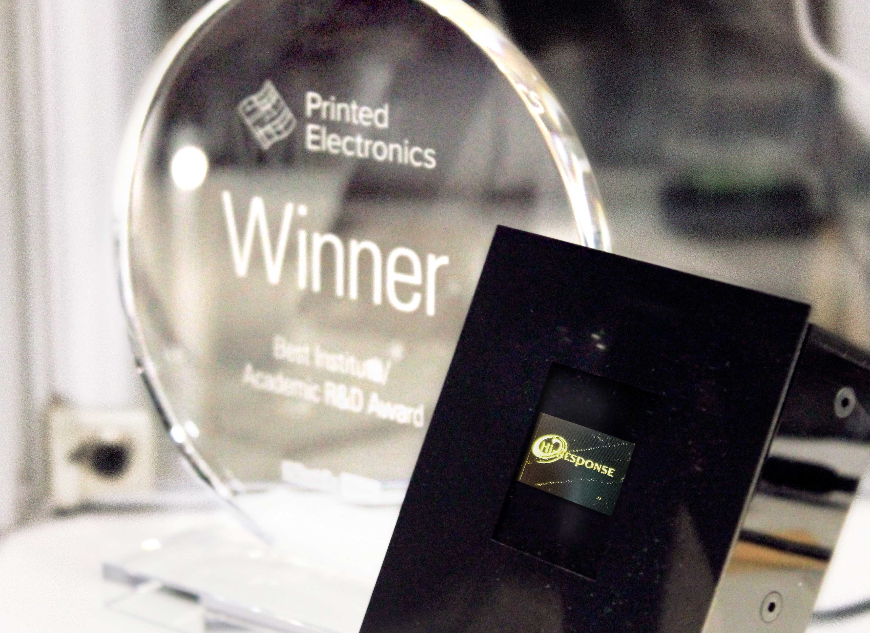
IDTechEX Printed Electronics Europe 2019: Best Institute / Academic R&D Award granted to consortium of Fraunhofer IAP, imec und TNO/Holst Centre
ESJET printing technology for large area active devices awarded
ESJET printing is a new printing technology for large-scale, solution-processed displays of the future. It enables higher resolution and drop on demand printing. The Potsdam Fraunhofer Institute for Applied Polymer Research IAP, together with its project partners imec and TNO/Holst Centre, has developed this printing technology for solution-processed displays of the future.
The Fraunhofer Institute for Applied Polymer Research IAP, imec and TNO/Holst Centre have been awarded with the Best Institute / Academic R&D Award at IDTechEx Printed Electronics 2019. The award is granted for “significant contribution over the past 24 months to the understanding of the principles and accrued knowledge behind printed electronics”, the guidelines state. Dr. Richard Collins, Senior Analyst at IDTechEx, presented the award on April 10th, 2019.
Within the EU project, Hi-Response, 13 consortium members are working together to develop a highly innovative Pulsed Electro-Static Printing Technology for high resolution printing for different applications. Within Hi-Response, the researchers of the Fraunhofer IAP, imec and TNO/Holst Centre have developed high-resolution ESJET (electrostatic jetting) printing for conductive and emissive polymers, which opens up new possibilities for various applications. The technology has the potential to be implemented for high-resolution printing of AM OLEDs with pixel sizes below 10 µm yielding in RGB resolutions beyond 500 ppi. This technology - being scalable - enables large area printing of active devices. Furthermore, the ESJET can deposit a much wider range of viscosities from 1 to 10,000 cP, compared to 1-40 cP for inkjet printers.
The advantages of the technology of ESJET printing
“With ESJET, we are able to significantly reduce pixel sizes for printed AM OLEDs”, Dr. Christine Boeffel, project manager at the Fraunhofer IAP says. “One of the remarkable things about the technology is that even at pitches of 25 µm, pixel sizes down to 10 µm are printable. For our demonstrator we printed 62967 single 10 µm wide dots to make a working display with a 300 ppi resolution.”
Imec and TNO/Holst Centre developed AM OLED backplanes and provided them to the Fraunhofer IAP for processing of the OLED front plane. High-resolution ESJET printing was implemented for the deposition of the PEDOT:PSS hole injection layer consisting of the print of 62967 single 10 µm wide dots on the 0.5 inch wide active matrix backplane. The subsequent layer of the emitting material was processed by spin coating followed by thermal evaporation of the transparent electrode.
“It is a great milestone to print OLED materials in such small dimensions. Improving in the printing resolution opens new possibilities for solution processed OLED display”, Dr. Tung-Huei Ke, senior researcher at imec says.
“We have reached an important goal getting the technology of ESJET printing this far. We are convinced that pixel sizes can be reduced even further below the mark of 10 µm. We plan to print OLED materials for RGB display applications at 300 ppi in future projects”, Dr. Manuel Gensler, researcher for ESJET printing at the Fraunhofer IAP says.
“With the display industry searching for new and innovative ways to increase display resolution as well as to include new user interfaces into the full display area, high-resolution printing technology is a key enabler to realize these goals by printing OLED materials as well as other functional materials at high resolution”, Dr. Auke Jisk Kronemeijer, GEN1 TFT Pilot Line Manager at TNO/Holst Centre says.
Last modified:
