Functional Materials and Devices


OVERVIEW


Technology development for organic electronics

The objective of the work on technology development for organic electronics devices is to realise intelligent systems in life science, automotive, textile and architectural applications, consisting of a combination of OLED, OPV, organic electronics, sensor and energy storage technologies. To this end, prototypical product ideas and production technology concepts will be implemented.


Nanomaterials and Quantum Dots

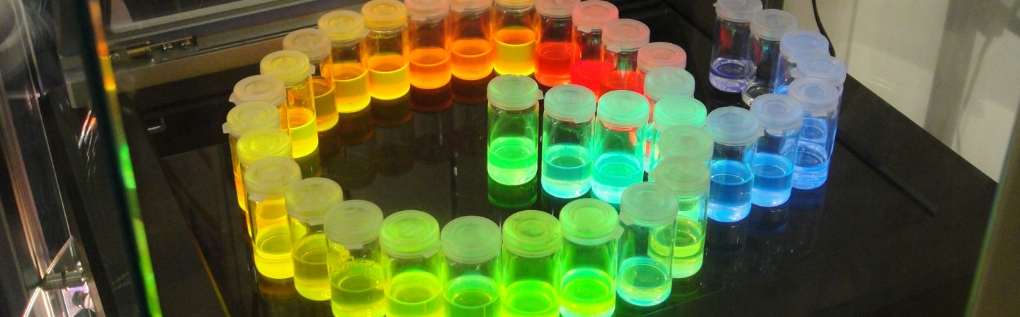
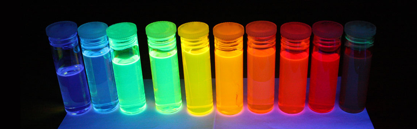
Quantum dots (QD) are a new class of nanomaterials in which the absorption and emission properties can be adjusted in a unique way. We are developing synthesis processes based on cadmium-free starting materials to provide environmentally friendly and RoHS compliant QDs, e.g. based on indium phosphide or zinc selenide, for QD LED and colour filter applications as well as for solar technology. In addition, new processes are being tested to scale up the synthesis of these materials to the gram scale.


Surface functionalisation and analysis

We develop technologies to adapt the properties of surfaces - especially those of polymers - to the requirements of an application. We have experience in very different areas. They range from the development of environmentally friendly pretreatment processes for an adhesive metallization to the functionalization of surfaces for use in biological quality control, the food industry and medical diagnostics. In addition, we have a wide range of analytical tools at our disposal to characterise surfaces.

Demonstrator | Printed organic thin-film solar cells (OPV)


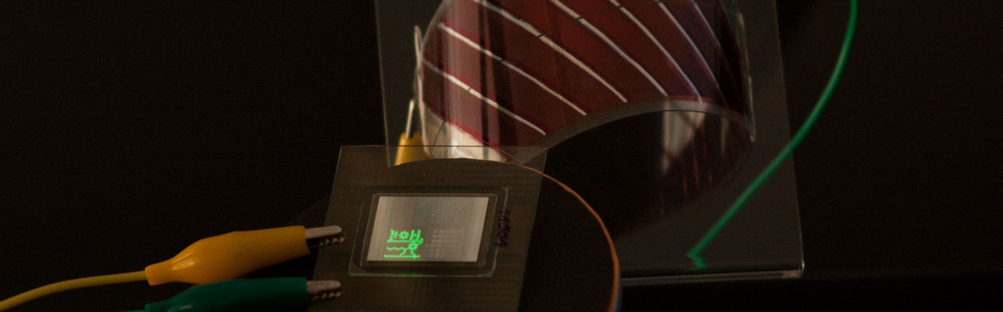
Our module consists of four printed organic thin-film solar cells, each with an area of 15 x 15 cm². The flexibility in form and design makes them particularly attractive for energy-efficient building. Beyond that, there are also almost unlimited possibilities for use. All processes are scalable, so that inexpensive mass production of the modules is possible.

Advantages

  • Low weight due to thin layers
  • Bendable foil substrates possible
  • Flexibility in form and design
  • Versatile application possibilities
  • Scalable processes enable low-cost mass production
 

Printed organic thin-film solar cells (OPV)

What we offer

  • Testing of new (OPV) materials and optimization of layer stacks
  • Formulation of printable inks
  • Characterization of the physicochemical properties of materials, layers and complete devices

  • Characterization of the ageing and durability of solar cells under various environmental influences
  • Customised OPVs for demonstrators and prototypes up to a substrate size of 150 x 150 mm
  • Complete solutions through comprehensive expertise and a network of technology partners

Demonstrator | Cadmium-free quantum dots


Quantum dots (QDs) are inorganic nanoparticles that have very special properties due to their small size. The luminescence is narrow-banded and can be adjusted over the entire colour spectrum. QDs have a wide range of applications and are used in many areas: as highly efficient light converters or brilliant light sources in displays, as light sources for illumination and as specific markers in sensor technology. 

Our specialization are cadmium-free quantum dots, which are less problematic for the environment and humans. These are based on indium and zinc. 

Possible applications

 
  • Solar concentrator
  • Colour converter for display and lighting
  • QD LEDs for display and lighting
  • Luminescent markers for analytical methods

What do quantum dots offer

 
  • Narrow band emission, adjustable via particle size
  • Strong optical absorption
  • Optically and electrically excitable

What we offer

  • Development and synthesis of quantum dots with tailored properties
  • Formulation of printable inks
  • Characterization of the photophysical properties and ageing of QDs in solution, as solid and in the device

  • Adaptation of the envelope structure of quantum dots for mixing into plastics and photoresists, for efficient charge carrier transfer in QD LEDs, for specific binding to proteins and sugars for biological applications
  • Components for demonstrators and prototypes

Demonstrator | QD-LEDs


We develop quantum dots (QDs) as emitters in displays and light sources. The QDs are directly electrically excited, the light source previously required to excite fluorescence is no longer necessary. Our innovative optoelectronic devices combine the advantages of OLEDs with the outstanding lighting properties of quantum dots: QD LEDs have the uniform light pattern, the paper-thin structure and the efficient operation of an OLED. At the same time, the wavelength of the light is freely adjustable and very narrow-banded.

The aim of our work is to further reduce manufacturing costs while optimising colour spectra and component efficiency. For display applications, we are aiming for the BT.2020 colour space. We deliberately avoid using toxic cadmium as a quantum dot material and thus obtain components that are less problematic for the environment and humans.

Light-emitting quantum dots for use in display technologies

  • Narrow band emission
  • Adjustable emission wavelength
  • Uniform illumination over the entire surface
  • Very thin to produce
  • Can be manufactured on flexible substrates
  • Energy-saving and efficient in operation
  • Low heat generation
  • Clear and distinct image from every angle
  • High potential for cost savings in liquid processing

What we offer


  • Development and synthesis of new quantum dot materials for display applications
  • Optimization of the layer stacks
  • Formulation of printable quantum dot inks
  • Analytical tests of the lifetime and durability of QD LEDs under various environmental influences
  • Customised QD-LED components for demonstrators and prototypes up to a substrate size of 50 mm x 50 mm

Demonstrator | Lighting technology from the printer: OLEDs


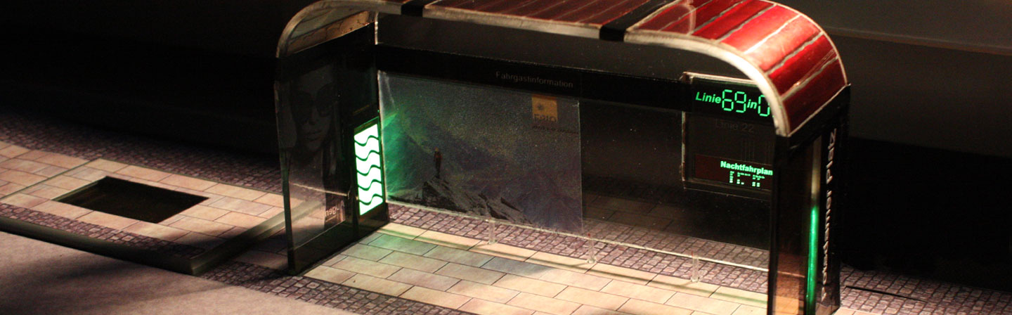
We develop organic light-emitting diodes (OLEDs) for ambient lighting and signage applications. OLEDs have a uniform luminance over the entire active surface. The result is a clear and distinct luminous image that is easily visible from any viewing angle. For ambient lighting applications, the active surface can have almost any geometrical shape.

  • Flush lighting over the entire surface
  • Can be produced very thin
  • Can be produced on flexible substrates
  • Energy-saving and efficient, low heat generation
  • A clear and unambiguous picture
  • High potential of cost savings (liquid processing)
 

Collaboration

Our specialisation is OLEDs with liquid processed printed layers. Up to now OLEDs for lighting purposes and displays have been produced by vapor deposition processes. However, the vacuum equipment required for this and changes in layout and size are associated with high costs. The production of vapour-deposited OLEDs is therefore only worthwhile for high volumes. The more layers of the OLED are printed, the higher the potential cost savings.

What we offer

  • Testing of new (OLED) materials and optimisation of layer stacks
  • Formulation of printable inks
  • Analytical tests of the physico-chemical properties of materials, layers and complete devices

  • Characterisation of the photophysical lifetime and durability of OLEDs under different environmental conditions
  • Customised OLEDs for demonstrators and prototypes up to a substrate size of 50 mm x 50 mm
  • Complete solutions through comprehensive expertise from the technology network GOTA - German OLED Technology Alliance
 

We can structure OLEDs flexibly. This opens up countless design possibilities. In contrast to inorganic LEDs, no diffuser is required, which makes paper-thin lighting elements on rigid or flexible substrates possible.

Typical applications of the energy-saving and efficient OLEDs are:

  • Architecture and interior design,
  • Automotive applications,
  • Signage or advertising.


They are mainly used where a low construction depth is required.

Demonstrator | AM-OLED


Liquid processing is a new trend in the production of OLED displays. According to the current state of the art, OLED materials are still mostly applied by vapor deposition processes. However, much material is lost on shadow masks and other surfaces. With printing processes, on the other hand, the ink can be applied specifically to the active pixel areas. A material efficiency of up to 90 % is possible for an RGB display. 

However, high-resolution displays are a challenge for printing processes. The smallest technically realised drop size in piezo-based inkjet printing is approximately 1 pL. This means that RGB displays can be printed at a maximum of 240 ppi. This is sufficient for television sets. For smartphones and microdisplay applications, however, a resolution of at least 500 ppi is required.

ESJET/EHDJET Technology

  • Very fine structures <10 µm in high resolution >500 ppi printable
  • Printing of low and high viscosity inks (1 - 10000 cP)
  • Digital printing (drop-on-demand) and vector-based printing (continuous jet) 


The AM-OLED demonstrator was realised in cooperation with imec and TNO / Holst Center. Hi-Response was funded under Grant Agreement No 646296 within the H2020 NMP Pilot 2014 Programme of the European Union.

What we offer

  • (Further) development of inks for electrostatic printing
  • Consulting and tests for new applications of the technology
  • Complete solutions through comprehensive expertise and a network of technology partners

We continue to develop the technology of electrostatic printing (ESJET/EHDJET) for printing high-resolution OLED displays. On a monochrome active matrix display we were able to demonstrate a resolution of 900 ppi ("Hi-Response"). The next step is coloured OLED or QD LED displays in RGB as well as the printing of colour filters for display applications.

Demonstrator | Liquid Processed OLED without vaporisation steps


In liquid-processed OLEDs, the extremely thin layers are applied by printing technologies. This eliminates the otherwise usual vapor deposition processes. Cost-intensive vacuum systems are not required. Liquid-processed OLEDs are a current trend in the production of displays. Here, the three active dyes (emitters) in red, green and blue are applied in a structured manner by inkjet or ESJET printing. However, all other layers, which are the same for all three dyes, are still applied by vapour deposition. 

We are developing OLEDs which can be produced without any vaporisation processes. OLEDs processed in this way still have a lower efficiency than their conventionally produced models. On the other hand, the investment costs are significantly lower, so that even small quantities can be produced economically. Furthermore, the printing processes can be adapted quickly and flexibly to changes in layout and form. Therefore, completely liquid-processed OLEDs are initially interesting for signage and advertising purposes.

Potential applications

 
  • Signage
  • Advertising purposes
  • Ambient lighting

What we offer

  • Completely liquid processed OLED without vaporisation steps
  • Development of cost-effective manufacturing processes
  • Flexible variation of design and layout through printing processes

Demonstrator | Particle-free silver complex ink for inkjet printing


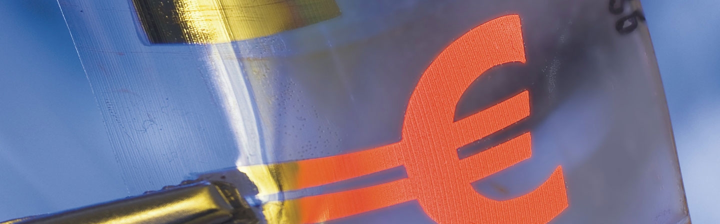
With a transparent complex ink, precise circuits of silver can be applied by inkjet printing. The ink is not particle-based, which on the one hand improves printability and on the other hand allows the processing of thinner layers by a lower loading of silver (< 5 %). Thermal curing is carried out at low temperatures (approx. 130 °C), which allows curing not only on glass (right) but also on sensitive surfaces such as foil or paper (left).

Potential applications

  • (Transparent) electrodes for OLEDs
  • Electrodes and supply lines for thin-film solar cells
  • Wearables
  • Printed electronics

What we offer

  • Comprehensive characterisation of inks
  • Tailor-made adaptation of ink formulations to printing processes
  • Process optimisation for printing conductive structures on various substrates
  • Further development for processing other metals (e.g. copper)

Demonstrator | Process control for silicone coatings

Quality control during the running process: We have developed a new method to enable the measurement of a transparent coating on a transparent film already during production. This involves introducing an organic fluorescent dye into the coating liquid, such as varnish or impregnation, which remains identifiable and measurable throughout the process.

Fluorescent organic dyes can be detected in very small quantities: even at a concentration in the range of a few ppm (parts per million, ratio 1 to 1 million), individual layers can be identified that are only a few micrometers thick. Moreover, the small quantities do not affect the properties of the starting material, such as strength.


The distribution of a coating layer thickness on a PET film was recorded at 3 m/min with a resolution in the range of mm.

Potential applications

  • Single layers in multi-layer films
  • Impregnations
  • (Organic) coatings
  • Laminating adhesive layers

Benefits of the procedure

  • Reduction of production costs
  • Improving product quality
  • In-line implementation
  • Application to different coating processes
  • Optimisation of the coating preparation process

OUR RANGE OF SERVICES


OLEDs

  • Tailor-made OLEDs for demonstrators and prototypes (e.g. for keyboards, signage, advertising, security applications)
  • Customer-specific development of applications with OLEDs
  • Process development: ink development, ITO-free OLEDs, transparent electrodes, flexible substrates, OLEDs without vacuum processes, process parameters
  • Determination of the barrier properties of substrates and encapsulation (calcium level test)
  • Encapsulation - rigid and flexible
  • Thin film encapsulation (Atomic Layer Deposition, ALD)
  • Tests of OLED materials, development and optimisation of OLED stacks
  • Complete solution for OLED production through comprehensive expertise from the technology network GOTA - German OLED Technology Alliance


Quantum dots (QD)

  • Development and synthesis of QDs with customised properties
  • Customer-specific development of applications with QDs: display technology, photovoltaics, LEDs and biology
  • Process development: ink development, mixing in plastics and photoresists, specific application to proteins and sugars, process parameters
  • QD-LEDs (optimisation of QD-LED stacks, production of components)
  • QD Photovoltaics
  • QD colour filter


Fluorescence collectors

  • Development of fluorescence collectors for solar technology with fluorescent dyes and quantum dots
  • Visible spectral range
  • NIR area


Solar cells

  • Customer-specific development of solar cells based on organic materials and perovskites - from single cells to application modules
  • For energy self-sufficient systems
  • Process development: ink development, process parameters


Electroluminescent displays

  • Prototype development for electroluminescent displays in sheet-to-sheet and roll-to-roll processes


Consulting and training

  • Process development, process equipment, process training
  • Consulting for development projects (infrastructures)
  • Further education and training


Plagiarism protection

  • Development of recipes for the protection against plagiarism of organic materials and products made from them


Surface and thin film technologies

  • Development of surface and thin film technologies for and with polymers
  • Surface treatment with low-pressure plasma, VUV radiation
  • Functionalisation of surfaces with gases and liquids


Contract analysis

  • Surface analysis (XPS, contact angle, profilometry, AFM, sheet resistance)
  • Climate tests (ambient: 23 °C/50 % r.h., tropical 38 °C/90 % r.h., accelerated 60 °C/90 % r.h., humid heat 85 °C/85 % r.h. or free on request)
  • Photophysical characterisation of materials (UV/Vis, fluorescence, EQE - external quantum efficiency, time-resolved luminescence)
  • Material properties (TGA - thermogravimetric analysis)

OUR EQUIPMENT


Thin Film Technologies

  • Plasma CVD (Chemical vapour deposition), laboratory to roll-to-roll
  • PVD (steaming, sputtering)
  • Spin-coating (inert and in atmosphere)


Printing Technologies

  • Ink Jet Printing (Pixdro LP50 inert and atmospheric, Dimatix, up to DIN-A4)
  • ESJET Printing (pilot plant for high-resolution printing)
  • Squeegee (Erichsen Coatmaster 510 with heatable table up to DIN-A4)
  • Slot die Coating (on Coatema Easy Coater for coating for formats up to 300 x 300 mm² and Mathis Slit Coater for formats up to 150 x 150 mm²)
  • Silkscreen
  • Roll-to-roll gravure printing
  • Pad printing


Process tools

  • Laminating unit for the encapsulation of rigid and flexible carriers
  • ALD (Beneq TFS 200 for formats up to 150 x 150 mm², thermal and plasma)
  • Steaming


Surface Technology

  • Various plasma systems, from laboratory scale to roll-to-roll in 30 cm width
  • VUV excimer spotlight for 3D parts and roll-to-roll in 30 cm width
  • Roll-to-roll system in 30 cm width with corona and printing technology for functionalising surfaces
  • Metallization equipment


Special measuring techniques

  • Visual
    • Hamamatsu Quantum Yield Measurement System
    • FLS920-stm (Edinburgh Instruments) with option for time-resolved measurements in the ns and µs to ms range (TCSPC, MCS)FT-IR Nexus 470 Thermo Scientific
      • Transmission 400 – 4000 cm-1
      • ATR 650 – 4000 cm-1
    • FT-IR IS20 Thermo Scientific
      • Transmission 400 – 7500 cm-1
      • Pike Gladiator ATR 525 - 7500 usable up to 200 °C; ramps and measuring intervals programmable
  • Electrical
    • Spectroradiometer for OLED characteristics (Konica-Minolta CS-2000)
    • 4-point measuring station for measuring film resistances
  • Microscopy
    • AFM (Nanosurf Easyscan 2)
    • 3D profilometry (Bruker Dektak XT)
  • Chemical
    • Functional group analysis on surfaces with XPS
    • Thermogravimetry (Mettler Toledo TGA 2)
    • Fluorescent labelling
  • Further
    • Calcium measuring station to determine the water vapour transmission through barrier layers
    • Determination of OLED lifetime (BoTest)
    • Measurement of solar cell characteristics (AM1.5)
    • Measurement of work function (Riken Keiki AC-2)

CONTACT

Armin Wedel

Contact Press / Media

Dr. Armin Wedel

Head of department | Functional materials and devices, QD development

Fraunhofer IAP
Geiselbergstraße 69
14476 Potsdam-Golm

Phone +49 331 568-1910

Christine Boeffel

Contact Press / Media

Dr. Christine Boeffel

OLED and OPV − Technology development

Fraunhofer IAP
Geiselbergstraße 69
14476 Potsdam-Golm

Phone +49 331 568-1915

Andreas Holländer

Contact Press / Media

Dr. Andreas Holländer

Surface functionality and analytics

Fraunhofer IAP
Geiselbergstraße 69
14476 Potsdam-Golm

Phone +49 331 568-1404

Manuel Gensler

Contact Press / Media

Dr. Manuel Gensler

Printing technologies

Fraunhofer IAP
Geiselbergstraße 69
14476 Potsdam-Golm

Phone +49 331 568-1913

Yohan Kim

Contact Press / Media

Dr. Yohan Kim

QD technologies

Fraunhofer IAP
Geiselbergstraße 69
14476 Potsdam-Golm

Phone +49 331 568-1924